Nanoelectronics and photonics
Introduction
- Nanoelectronics and photonics (NEP) involve the synthesis, fabrication and applications of semiconductor-based nanostructure materials and devices.
- The unique electrical and optical properties of nanostructures result in improved electrical performance and novel optical characteristics.
- These NEP devices increase the fundamental operating limits of, and open new windows of opportunities for, applications in optoelectronics, telecommunications and biomedical industries.
Vision
We focus on the the engineering of III-V compound semiconductors into various nanostructures
– quantum dots
– quantum dot molecules
– quantum wells
– quantum rings
Using molecular beam epitaxy, these quantum structures are routinely grown at sub-monolayer thicknesses and precisions, allowing electronic and photonic properties to be engineered at the material level.
Courses:
2102506
2102580*
2102582
2102583*
2102587*
2102589
2102663
2102682
Finite Element Analysis for Electrical Engineers
Semiconductor Technology: Fabrication and Characterization
Photonic Devices in Optical Communication Systems
Introduction to Quantum Mechanics
Sensor Technology and Applications
Laser Engineering
Solar Cell Technology
Solid-State Physics for Electronics Engineers
(3 Credits)
(3 Credits)
(3 Credits)
(3 Credits)
(3 Credits)
(3 Credits)
(3 Credits)
(3 Credits)
Example of Research Theme
Title 1. Infrared material engineering based on GaAsPBi compound semiconductorsDescription 1. Group III-V compound semiconductors have appropriate bandgap energies covering applications in the near-infrared (NIR) and mid-infrared (MIR) wavelengths. These compounds are grown and studied in our lab using molecular beam epitaxy (MBE) and characterisation techniques such as atomic force microscopy, photoluminescence. They find uses in optoelectronics, telecomms, and detectors.
Title 2. Irradiated Si pin photodiodes and their performances Description 2. Silicon photodiodes are used extensively in daily applications such as remote control receivers and other signalling systems. They are also used in specialized applications such as high-energy physics (HEP) experiments, particularly CMS at CERN. Our lab recently launched an initiative to study the degraded performance of these photodiodes after they have been bombarded by high-energy particles particularly neutrons (in collaboration with Thailand Institute of Nuclear Technology).
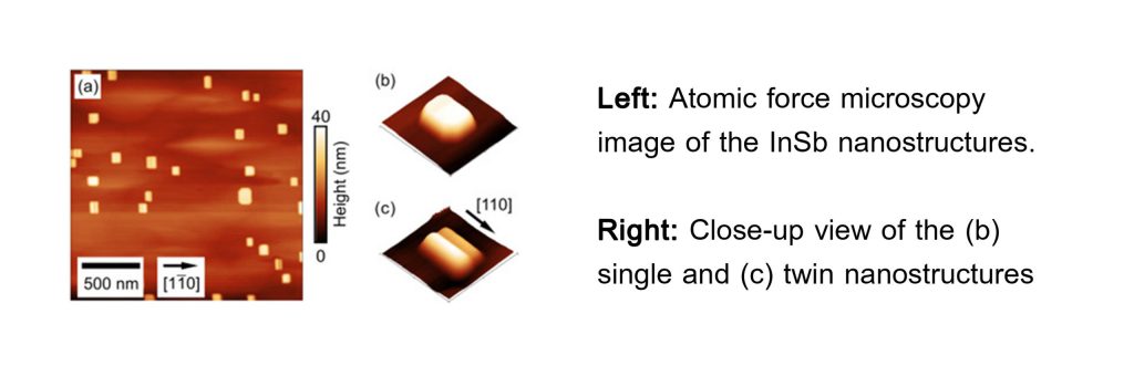
Title: Growth of truncated pyramidal InSb nanostructures on GaAs substrate
Description: This work shows the realization of truncated pyramidal InSb/GaAs nanostructures. Phenomenological growth model is developed based on the structural observation. These structures are infrared active and can be fabricated into photodetectors and emitters.
Microfluidic Devices
Introduction
- Microfluidics is related to the study and manipulation of small fluid volumes, ranging from pL to mL.
- Microfluidics is multiple disciplinary. For example, it involves mechanical, electrical, chemical and micro-/nano-engineering.
- Microfluidic devices can be widely applied to various fields including material sciences, food engineering, biotechnology, microbiology, biomedical engineering, etc.
- Due to small dimensions of fluid, the devices are fast, high sensitivity, economical.
Vision
We focus on the use of soft lithography to fabricate microfluidic devices for the research applications. Current fields of interest include
– On-chip microscale impedance measurement
– Droplet generation and manipulation.
– Plant cell manipulation.
– Cell/particle sorting and analysis
Our aim is to widen the microfluidic applications, not limited to electrical engineering, to be the grounds of advanced research in various field for the country and region.
Example of Research Theme
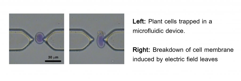
Title: Vacuole Isolation of Plant Cells
Description: Vacuole is an organelle mainly found in plant cells. The extraction of substances such as anthocyanins or pigments in the vacuole are of interest both in academic and in industrial aspects. A microfluidic device is designed to induce breakdown on cell membrane by applying electric field and obtain plant vacuole intact.
Cluster Coordinator

Advance Materials and Devices (AMD)
Songphol Kanjanachuchai
Songphol.k@chula.ac.th
Advance Materials and Devices (AMD)
Suwit Kiravittaya
suwit.ki@chula.ac.th
| Professor in the Cluster | Research Interests |
| Songphol Kanjanachuchai [SKJ] | semiconductors, microelectronics, crystal growth, surfaces and interfaces |
| Duang-rudee Worasucheep [DWC] | Optical fiber communication, Optoelectronics, Wavelength division multiplexing, High-speed optical transceiver, Access optical network, Semiconductor optical amplifier, Erbium doped fiber amplifier |
| Chanchana Tangwongsan [CTS] | Synthesis of nano particles for various applications, Biomedical instrumentation |
| Chanin Wissawinthanon [CWN] | Photonics / Nanophotonics, Optoelectronics, Semiconductor science and technology, Optical / Laser metrology |
| Suwit Kiravittaya [SKY] | Photonics, Electronics, Solar Cell, Photodetector, LED, Light Emitting Diode, Laser, Molecular Beam Epitaxy, Optical Properties, Semiconductor, Nanostructure, Quantum Technology, Quantum Sensing, Quantum Secure Communication, Quantum Computing |
| Boonchai Techaumnat [BTA] | High-voltage engineering, Transmission-line technologies, Numerical field analysis, Particle Electromechanics Powder technologies, Micro-Nano engineering, Lab-on-a-Chip / Microfluidics, Bioelectromagnetic |
| Chalermchai Himwas [CHW] | semiconductors, microelectronics, crystal growth, surfaces and interfaces |
| Hoang Luong | Semiconductors |